- 您现在的位置:买卖IC网 > Sheet目录312 > AT26DF081A-SSU (Atmel)IC FLASH 8MBIT 70MHZ 8SOIC
�� �
�
�5.� Device� Operation�
�The� AT26DF081A� is� controlled� by� a� set� of� instructions� that� are� sent� from� a� host� controller,� com-�
�monly� referred� to� as� the� SPI� Master.� The� SPI� Master� communicates� with� the� AT26DF081A� via�
�the� SPI� bus� which� is� comprised� of� four� signal� lines:� Chip� Select� (CS),� Serial� Clock� (SCK),� Serial�
�Input� (SI),� and� Serial� Output� (SO).�
�The� SPI� protocol� defines� a� total� of� four� modes� of� operation� (mode� 0,� 1,� 2,� or� 3)� with� each� mode�
�differing� in� respect� to� the� SCK� polarity� and� phase� and� how� the� polarity� and� phase� control� the�
�flow� of� data� on� the� SPI� bus.� The� AT26DF081A� supports� the� two� most� common� modes,� SPI�
�modes� 0� and� 3.� The� only� difference� between� SPI� modes� 0� and� 3� is� the� polarity� of� the� SCK� signal�
�when� in� the� inactive� state� (when� the� SPI� Master� is� in� standby� mode� and� not� transferring� any�
�data).� With� SPI� modes� 0� and� 3,� data� is� always� latched� in� on� the� rising� edge� of� SCK� and� always�
�output� on� the� falling� edge� of� SCK.�
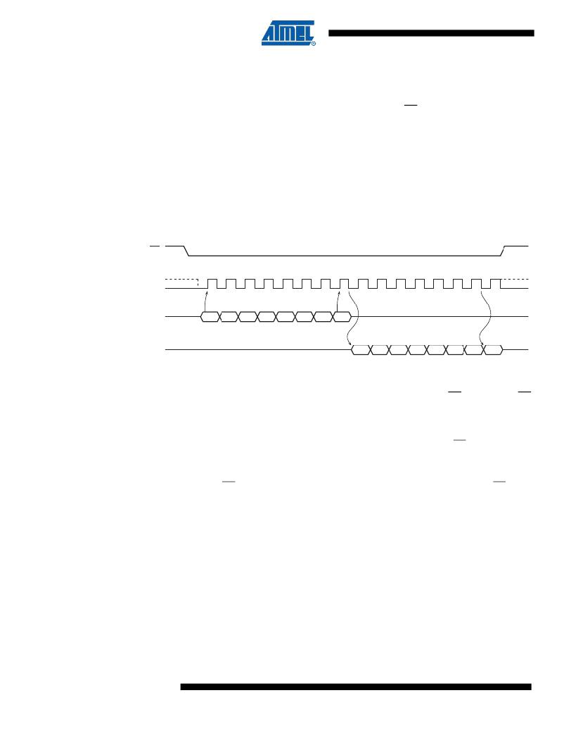
�Figure� 5-1.�
�C� S�
�S� CK�
�SPI� Mode� 0� and� 3�
�S� I�
�M� S� B�
�L� S� B�
�S� O�
�M� S� B�
�L� S� B�
�6.� Commands� and� Addressing�
�A� valid� instruction� or� operation� must� always� be� started� by� first� asserting� the� CS� pin.� After� the� CS�
�pin� has� been� asserted,� the� SPI� Master� must� then� clock� out� a� valid� 8-bit� opcode� on� the� SPI� bus.�
�Following� the� opcode,� instruction� dependent� information� such� as� address� and� data� bytes� would�
�then� be� clocked� out� by� the� SPI� Master.� All� opcode,� address,� and� data� bytes� a� re� transferred� with�
�the� most� significant� bit� (MSB)� first.� An� operation� is� ended� by� deasserting� the� CS� pin.�
�Opcodes� not� supported� by� the� AT26DF081A� will� be� ignored� by� the� device� and� no� operation� will�
�be� started.� The� device� will� continue� to� ignore� any� data� presented� on� the� SI� pin� until� the� start� of�
�the� next� operation� (CS� pin� being� deasserted� and� then� reasserted).� In� addition,� if� the� CS� pin� is�
�deasserted� before� complete� opcode� and� address� information� is� sent� to� the� device,� then� no� oper-�
�ation� will� be� performed� and� the� device� will� simply� return� to� the� idle� state� and� wait� for� the� next�
�operation.�
�Addressing� of� the� device� requires� a� total� of� three� bytes� of� information� to� be� sent,� representing�
�address� bits� A23� -� A0.� Since� the� upper� address� limit� of� the� AT26DF081A� memory� array� is�
�0FFFFFh,� address� bits� A23� -� A20� are� always� ignored� by� the� device.�
�6�
�AT26DF081A�
�3600G–DFLASH–06/09�
�发布紧急采购,3分钟左右您将得到回复。
相关PDF资料
AT26DF161-SU
IC FLASH 16MBIT 66MHZ 8SOIC
AT26DF161A-MU
IC FLASH 16MBIT 70MHZ 8QFN
AT26DF321-SU
IC FLASH 32MBIT 66MHZ 8SOIC
AT27BV010-90JU
IC OTP 1MBIT 90NS 32PLCC
AT27BV020-90JU
IC OTP 2MBIT 90NS 32PLCC
AT27BV040-12JU
IC OTP 4MBIT 120NS 32PLCC
AT27BV1024-90JU
IC OTP 1MBIT 90NS 44PLCC
AT27BV256-70JU
IC OTP 256KBIT 70NS 32PLCC
相关代理商/技术参数
AT26DF081A-SSU-RET
制造商:Atmel Corporation 功能描述:
AT26DF081A-ST-B
制造商:Adesto Technologies Corporation 功能描述:8-SOIC-W, AUTO GRADE 3, 2.7V, TUBE - Rail/Tube
AT26DF081A-ST-T
制造商:Adesto Technologies Corporation 功能描述:8-SOIC-W, AUTO GRADE 3, 2.7V, T&R - Tape and Reel
AT26DF081A-SU
功能描述:闪存 8M 8 I/O Pins SPI 256B 2.7V-3.6V RoHS:否 制造商:ON Semiconductor 数据总线宽度:1 bit 存储类型:Flash 存储容量:2 MB 结构:256 K x 8 定时类型: 接口类型:SPI 访问时间: 电源电压-最大:3.6 V 电源电压-最小:2.3 V 最大工作电流:15 mA 工作温度:- 40 C to + 85 C 安装风格:SMD/SMT 封装 / 箱体: 封装:Reel
AT26DF081-MU
制造商:Adesto Technologies Corporation 功能描述:SF DATAFLASH, 8M, MLF, IND TEMP,GREEN - Trays
AT26DF081-SU
制造商:Adesto Technologies Corporation 功能描述:SF DATAFLASH, 8M, SOIC ,IND TEMP, GREEN - Rail/Tube
AT26DF161
制造商:ATMEL 制造商全称:ATMEL Corporation 功能描述:16-megabit 2.7-volt Only Serial Firmware DataFlash Memory
AT26DF161_06
制造商:ATMEL 制造商全称:ATMEL Corporation 功能描述:16-megabit 2.7-volt Only Serial Firmware DataFlash Memory